The Leading Qualified Medical Device Supplier Directory
Discover + Source + Connect


Discover Qualified Suppliers You Can Trust
With the Qmed+ directory, you can trust you'll be connected with qualified suppliers, service providers, and consultants to the medtech industry that meet global standards for current good manufacturing practice (cGMP) regulations and quality management systems (QMS). In order to be considered for inclusion in the Qmed+ supplier directory, companies must show qualification through these criteria or proven experience working with medical device manufacturers.


Featured Products
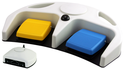
RF Wireless Foot Switch
Linemaster Switch CorporationLinemaster's RF Wireless foot control is a unique plug and go system perfect for new applications or as a replace...

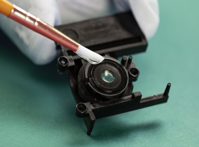
EP30-4Med: Optically Clear Epoxy Passes ISO 10993-5 Certification for Cytotoxicity
Master Bond Inc.Master Bond EP30-4Med&nb...

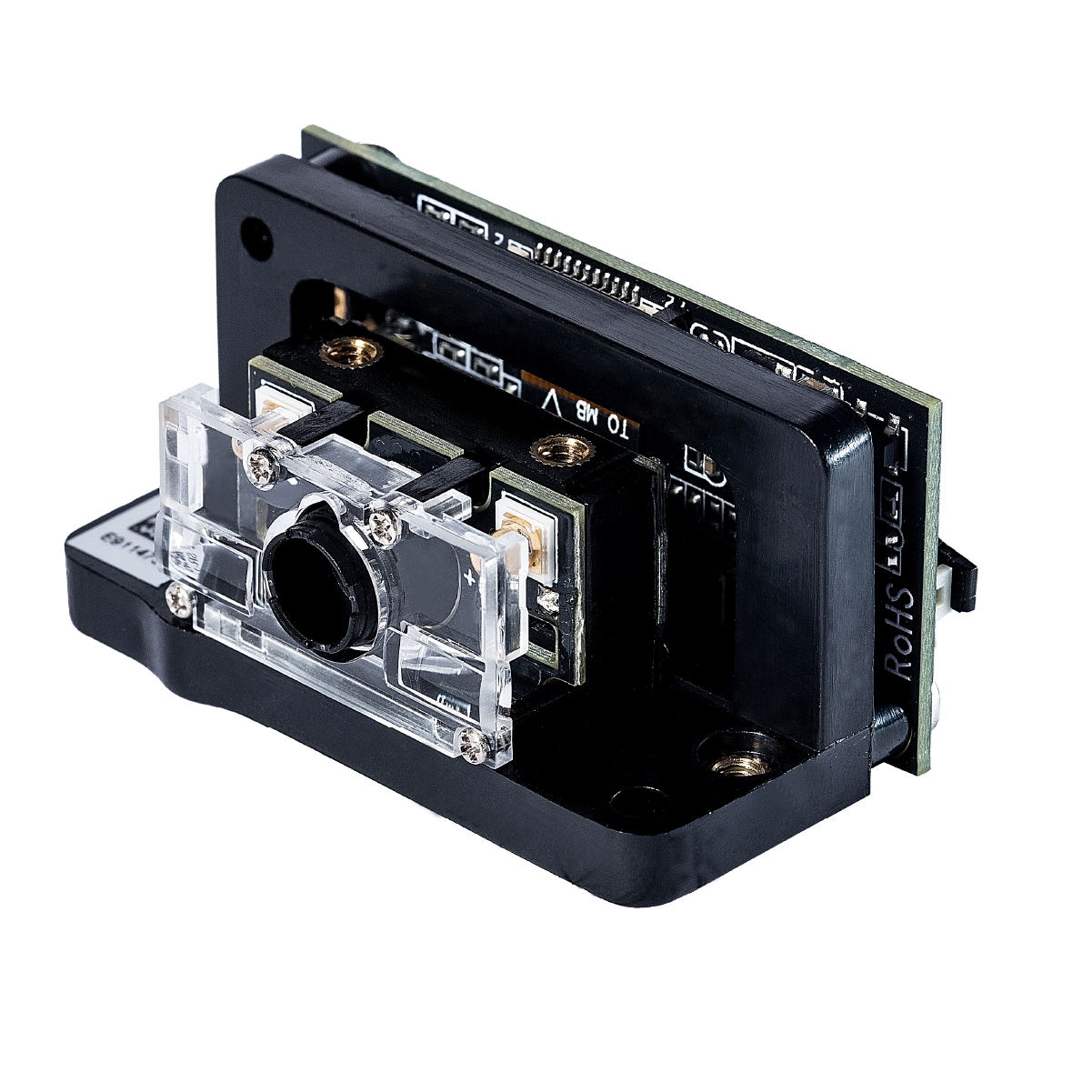
NLS-EM2037
Newland AIDC• Support 1D / 2D barcodes & Postal codes• Operating temperature: -20° to 60°C (-4°F to 140°F) • Size: 39.5(L) x 25.4(W) x 20.0...
%20x%20143%20(h)-comp304533.png)
Nitinol Processing
AMETEK Engineered Medical ComponentsNitinol is a two-element metal alloy utilized for many medical device applications due to its extraordinary properties...

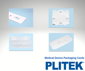
Medical Packaging Cards
Plitek, LLCPLITEK® manufactures a variety of medical packaging / backer cards for many medical applications. Utilizing ISO C...


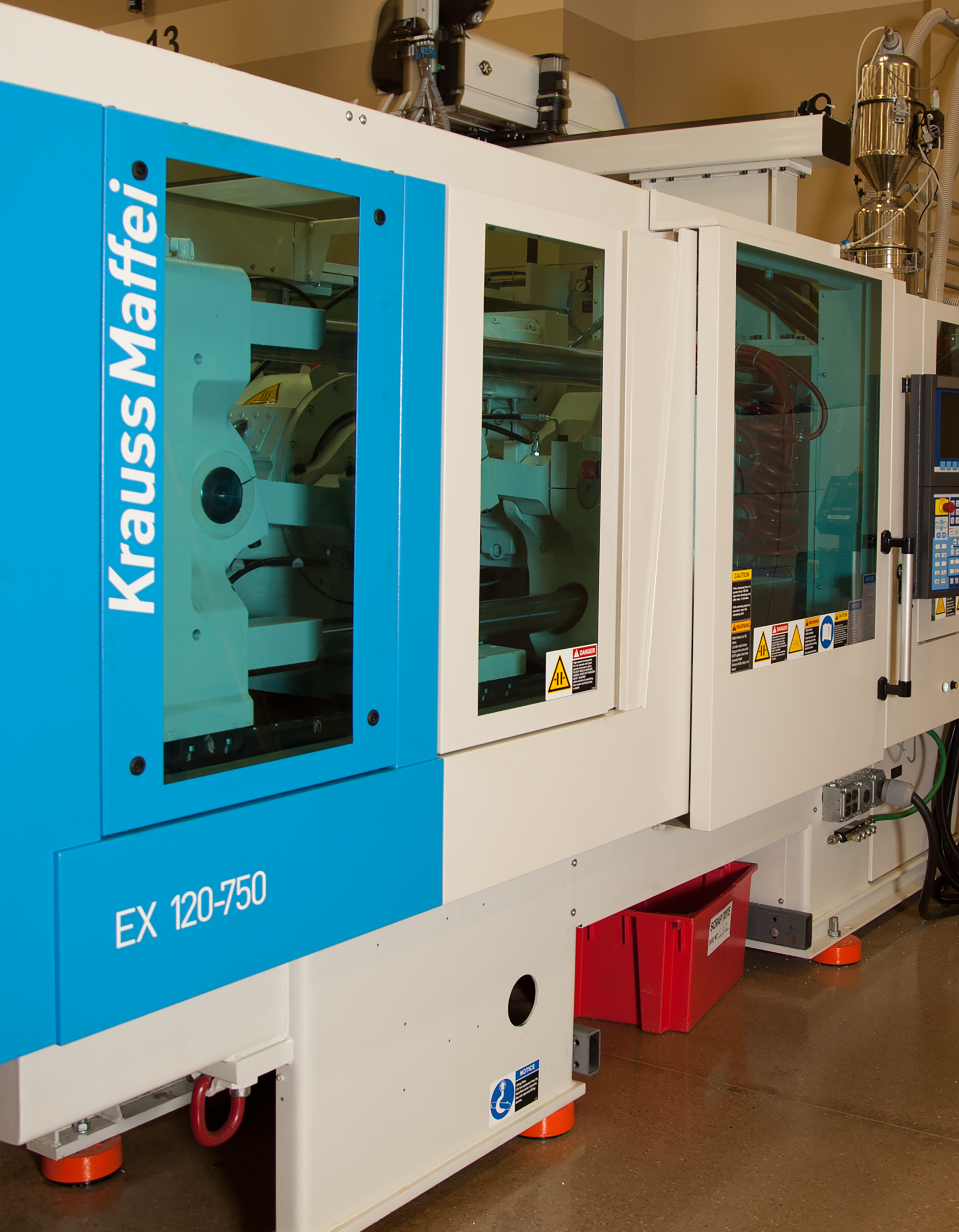
Custom Injection Molding
HTI PlasticsMaterials:We can run all types of resins from commodity to engineered grades, high temperature to filled materi...
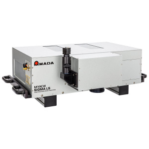
SIGMA LS Micromachining Subsystem
AMADA WELD TECHThe SIGMA LS Laser Micromachining Subsystem is a laser-integrated micromachining module desi...
Featured Companies


The Qmed+ directory simplifies and accelerates the new supplier research and discovery process. And it's easy to find exactly what you need: Search suppliers to the medical device industry by keyword or by product or service category.
Within each supplier's directory listing, you'll find a comprehensive company overview, contact information, qualifications, products and capabilities, supplemental resources, and ways to connect.
Discover and contact thousands of pre-qualified suppliers to the medical device and in vitro diagnostics industry. Start your sourcing journey now!
Medical device and diagnostics manufacturing is a fast-moving and highly regulated industry. Today, new and exciting technologies are enabling the creation of innovative medical products that are improving patient care by leaps and bounds. At the same time, the global web of regulatory requirements governing how those products are designed, developed, and produced is growing ever more complex. As a result, it’s becoming less and less likely that individual medical technology manufacturers have all the experience and capabilities they need—from design and development to manufacturing and regulatory affairs—in house.
Medical device manufacturers today can’t do it all themselves, so they must turn to outsourcers—design firms, testing labs, contract manufacturers, component and equipment suppliers, and consulting firms—to help bring their innovations to market. But finding trusted partners in the scattered landscape of medtech suppliers and service providers is no small task.
That’s why we created Qmed, the world’s only directory of pre-qualified suppliers and service providers to the medical device and diagnostics industry. For nearly a decade, Qmed’s powerful search tool and online directory have enabled medtech manufacturers to connect with relevant partners that can help fill the gaps in their current capabilities and help speed their life-saving and -improving medical devices to market.
When medical device manufacturers turn to the Qmed directory for help in finding qualified outsource partners, they can trust they’ll be connected with suppliers, service providers, and consultants that meet global standards for good manufacturing practice and quality control, and which have relevant experience in the complex and evolving medtech industry.
In order to be considered for inclusion in the Qmed directory, companies must show qualification through some of the following criteria:
- ISO 9001 certification
- ISO 13485 certification
- CGMP compliance
- FDA registration
- Demonstrated experience with clients in the medical device or in vitro diagnostics space
Supplier News

Qosina Welcomes New Representative in Korea
QosinaQosina is pleased to announce the addition of David Oh as the new representative fo...

Trelleborg Breaks Ground on New Facility in Costa Rica
Trelleborg Healthcare and MedicalTrelleborg Healthcare & Medical breaks ground on a 107,600 square ...

Nick Lucka Promoted to Service & Support Manager
Enercon Industries Corp.Enercon Industries Corporation announces he promotion of Nick Lucka to th...
KNF Expands Smooth Flow Series of Diaphragm Pumps
KNF Neuberger, Inc.Pump manufacturer broadens its offering of innovative low pulsation line

Beacon MedTech Solutions Hires Henri Asselin to Lead Engineering Team
Beacon MedTech SolutionsBeacon MedTech Solutions is pleased to annou...
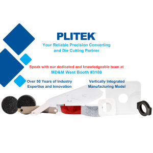
Visit PLITEK at MDM West booth 3180 - Precision Die Cutting and Converting
Plitek, LLCAre you facing manufacturing challen...
XBiotech Cures Shopfloor Management Woes with Cetec ERP
Cetec ERPXBiotech launches a new ultra-low-cost Cetec ERP manufacturing an...

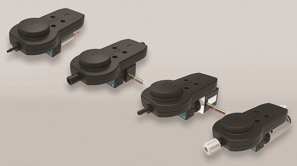
Drive systems for the laboratory automation
maxonReliability, precision and speed play key roles: maxon motors and drive systems are...
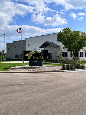
ProMed Molded Products opens new development and innovation facility
ProMed Molded ProductsProMed Molded Products announces the opening ...
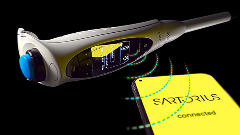
The New Picus® 2 Sets a New Standard for Connected Electronic Pipettes
Sartorius CorporationThe Life Science Group Sartorius introduce...
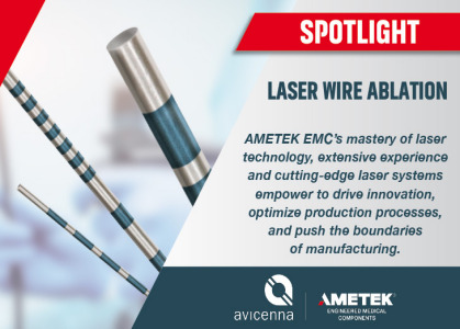
AMETEK EMC's Expertise in Laser Ablation of Fine Wires
AMETEK Engineered Medical ComponentsIn the realm of advanced manufacturing and precision engineering, ...
Ultra-Low Viscosity, Biocompatible Epoxy Offers Optical Clarity
Master Bond Inc.Master Bond EP4CL-80Med is a one part, optically clea...